In February 2004 Intel formally announced four new processors, built on the company’s industry-leading, high-volume 90 nanometre manufacturing technology. Formerly codenamed Prescott, the new processors were clocked at between 2.8 and 3.4GHz and differentiated from the previous Northwood series by an E designation. The expectation is for chips based on the Prescott core to have reached clock speeds of 4GHz by the end of 2004.
Initially, Prescott CPUs will use the same Socket 478 interface as earlier Pentium versions, run on the 800 MHz FSB, support Hyper-Threading and are compatible with a number of current Intel chipsets, such as the i875P and i865 family. The new core is expected to subsequently move to the LGA775 interface (also referred to as Socket T). This uses a land grid array of 775 pinouts and is a much cheaper form of packaging than either PGA or BGA.
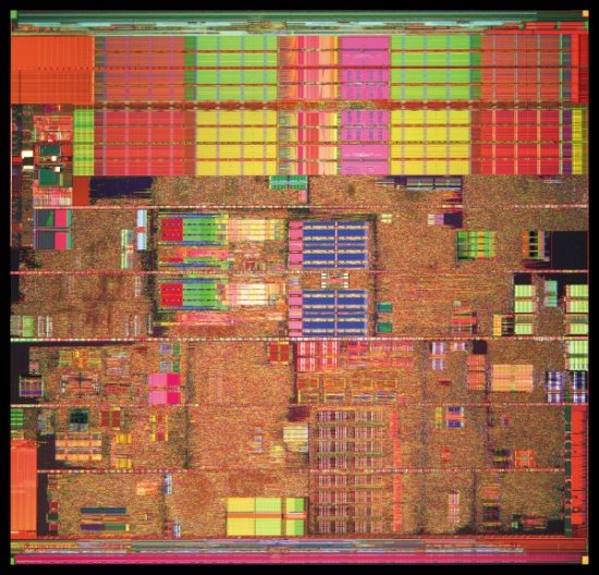
The Prescott’s major differences from its predecessor are its significantly deeper stage pipeline, increased cache sizes and an enhanced SSE instruction set. Compared with its predecessor, the Prescott’s pipeline has an additional 11 stages. The effect of a 31-stage pipeline will be to afford far greater headroom for faster clock speeds in the future. The size of both the L1 and L2 caches have been doubled to 16KB 8-way set associative and 1MB respectively, and the new core has 13 more SSE instructions – now referred to as SSE3 – than the Northwood.
Built exclusively on 300 mm wafers, Intel’s 90nm process technology combines high performance, low-power transistors, strained silicon, high-speed copper interconnects and a new low-k dielectric material. The new processors represent the first time all of these technologies have been integrated into a single manufacturing process. The Prescott core is also Intel’s first to have 7 metal layers, the additional layer being necessitated by the big increase in the new CPU’s transistor count, 125 million compared to the Northwood’s 55 million. Despite this, at 112mm2 the new 90nm Prescott core is more than 20% smaller than its predecessor.
Shortly after the launch of its initial line-up of Prescott-based CPUs, Intel also signalled that its future LGA775-based Prescotts (as well as its next-generation 32-bit Xeon processors) will include 64-bit x86 extensions that are compatible with AMD’s 64-bit architecture. While this tacit endorsement of its 64-bit technology initiatives can be seen as a victory for AMD – and a potential indictment against Intel’s own 64-bit Itanium 2 processors – it might also spell trouble for Intel’s rival in the longer term, by forcing AMD’s 64-bit processor line to compete on price, rather than technology.
Shortly after its decision to switch from clock speed to CPU processor numbers to denote relative performance and market positioning, Intel announced the first desktop processors to use the new 5xx model nomenclature in the summer of 2004. The new chips all used the company’s new PCI Express capable chipsets and LGA775 CPU interface and were equipped with 1MB of Level 2 cache. Clock speeds ranged from 2.8GHz for the model 510 to 3.6GHz for the model 560.
The final revision of the Pentium 4 was Cedar Mill, released in early 2006. This was simply a straight shrink of the 600-series core to 65nm, with no real feature additions. The table below shows the various incarnations of the Pentium 4 up until this final version of the mainstream desktop processor:
| Date | Codename | Transistors | Die
Size |
L2
Cache |
Fabrication | Speed
(GHz) |
|---|---|---|---|---|---|---|
| 2000 | Willamette | 42,000,000 | 217mm2 | 256KB | 0.18µm | 1.4 to 2.0 |
| 2002 | Northwood | 55,000,000 | 146mm2 | 512KB | 0.13µm | 2.0 to 3.4 |
| 2004 | Prescott | 125,000,000 | 112mm2 | 1MB | 0.09µm | to 3.6 |
| 2006 | Cedar Mill | 188,000,000 | 81mm2 | 2MB | 65nm | to 3.6 |
- Pentium Architecture
- Pentium Pro
- Pentium MMX Technology
- Pentium II
- Pentium SEC
- Pentium “Deschutes
- Pentium Xeon
- Pentium III
- Pentium Tualatin
- Pentium 4
- Pentium Northwood
- Hyper-Threading Technology
- Pentium Prescott
- Pentium Processor Numbers
- Multi-Core Processors
- Pentium Smithfield
- Pentium D
- Pentium Roadmap