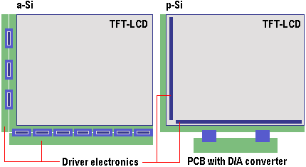
The thin-film transistors which drive the individual cells in the overlying liquid crystal layer in traditional active-matrix displays are formed from amorphous silicon (a-Si) deposited on a glass substrate. The advantage of using amorphous silicon is that it doesn’t require high temperatures, so fairly inexpensive glass can be used as a substrate. A disadvantage is that the non-crystalline structure is a barrier to rapid electron movement, necessitating powerful driver circuitry.
It was recognised early on in flat-panel display research that a crystalline or polycrystalline (an intermediate crystalline stage comprising many small interlocked crystals – analogous to a layer of sugar) of silicon would be a much more desirable substance to use. Unfortunately, this could only be created at very high temperatures (over 1,000oC), requiring the use of quartz or special glass as a substrate. However, in the late 1990s manufacturing advances allowed the development of low-temperature polysilicon (p-Si) TFT displays, formed at temperatures around 450oC. Initially, these were used extensively in devices which required only small displays, such as projectors and digital cameras.
One of the largest cost elements in a standard TFT panel is the external driver circuitry, requiring a large number of external connections from the glass panel, because each pixel has its own connection to the driver circuitry. This requires discrete logic chips arranged on the kitted pcb parts around the periphery of the display, limiting the size of the surrounding casing. A major attraction of p-Si technology is that the increased efficiency of the transistors allows the driver circuitry and peripheral electronics to be made an integral part of the display. This considerably reduces the number of components for an individual display – Toshiba estimates 40% fewer components and only 5% as many interconnects as in a conventional panel. The technology will yield thinner, brighter panels with better contrast ratios, and allow larger panels to be fitted into existing casings. Since screens using p-Si are also reportedly tougher than a-Si panels, it’s possible that the technology may allow the cheaper plastic casings used in the past – but superseded by much more expensive magnesium alloy casings – to stage a comeback.

By 1999, the technology was moving into the mainstream PC world, with Toshiba’s announcement of the world’s first commercial production of 8.4in and 10.4 in low-temperature p-Si (LTPS) displays suitable for use in notebook PCs. The next major advance is expected to see LTPS TFTs deposited on a flexible plastic substrate – offering the prospect of a roll-up notebook display!
- VA – Vertically Aligned LCD Monitors
- What in the LCD is IPS!?
- ThinCRT Flat Panels
- TFT LCD Monitors
- LCD Resolutions and Picture Scaling
- Liquid Crystal Light Polarisation in LCD Monitors
- Polysilicon Flat Panels
- Plasma Flat Panels
- PALCD Flat Panels
- OLED Flat Panels
- MVA – Multi-domain Vertical Alignment in LCD Monitors
- LEP Flat Panels
- LED Flat Panels
- LCD – Liquid Crystal Displays
- IPS – In-Plane Switching LCD Monitors
- HAD Flat Panels
- Flat Panel Feature Comparisons
- FED Flat Panels
- Digital Flat Panels
- DSTN LCD monitors
- Creating Colour in LCD Displays
- Flat Panel ALiS Technology