In 1971, Intel’s first processor – the 4004 – had 2,300 transistors. Thirty years later, the Pentium 4 had about 42 million. During that time chip makers’ basic strategy for making processors faster has been to shrink transistors to enable them to operate at higher frequencies and to enable more complex circuits to be packed onto a silicon die. However, as semiconductors have become ever more complex and new milestones in transistor size and performance have been achieved, power consumption and heat have emerged as limiting factors to the continued pace of chip design and manufacturing. The application of existing designs to future processors is unworkable because of current leakage in the transistor structure, which results in increased power consumption and the generation more heat.
In late 2002, Intel Corporation announced that its researchers had developed an innovative transistor structure and new materials that represented an important milestone in the effort to maintain the pace of Moore’s Law, and that would lead to a dramatic improvement in transistor speed, power efficiency and heat reduction. The new structure has been dubbed the Intel TeraHertz transistor because of its ability to be switched on and off more than one trillion times per second. The company hopes to eventually manufacture chips with more than a billion transistors – more than 10 times faster than, and fabricated with 25 times the density of transistors of the most advanced chips available in the early 2000s. Achieving this will mean that some chip elements will measure as little as 20nm wide – 1/250th the width of a human hair!
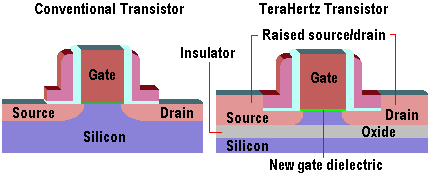
The transistor is a simple device built on a wafer of silicon that functions as an electronic on/off switch. Conventional transistors have 3 terminals: the gate, source and drain. The source and drain are variants of the basic silicon and the gate is a material called polysilicon. Below the gate is a thin layer called the gate dielectric, made of silicon dioxide. When voltage is applied to the transistor, the gate is on and electricity flows from source to drain. When the gate is off, there is no flow of electricity.

Intel’s TeraHertz transistor will contain three major changes. First, the transistors will feature thicker source and drain regions, substructures inside individual transistors that allow electrical current to pass. Second, an ultra-thin silicon insulating layer will be embedded below the source and drain. This is different from conventional silicon-on-insulator (SOI) devices, being fully depleted to create maximum drive current when the transistor is turned on, thereby enabling the transistor to switch on and off faster. The oxide layer also blocks unwanted current flow when the transistor gate is off. Third, the chemical composition of the gate oxide – the layer that connects the transistor gate to the source and drain – will be changed to a new high-k gate dielectric material, grown using a technology called atomic layer deposition, in which growth occurs in layers one molecule thick at a time. The precise chemical composition of the gate oxide has yet to be decided, candidates including oxides from aluminium and titanium, amongst others.
All three improvements are independent but work toward the same goal: allowing transistors to use electricity more efficiently:
- Thickening the source and drain regions and changing the chemical composition of the gate oxide will help stem gate leakage, current that leaks out of the gate. The smaller transistors get the more current escapes from them, forcing designers to pump in even more electricity, which in turn generates even more heat. Intel claims the new material will reduce gate leakage more than 10,000 times compared with silicon dioxide.
- The addition of the SOI layer will also lower resistance to the flow of current across the source and drain. Ultimately, lower resistance will allow designers to either lower power consumption or improve performance at a given level of energy.
- Other benefits are also likely to appear. For example, free-floating alpha particles that come in contact with a transistor on current chips can switch a transistor’s state unexpectedly and cause errors. In the future, these will be absorbed by the ultra thin SOI layer.
Current Pentium 4 processors run at 45 Watts; the aim is for the TeraHertz transistor to enable power dissipation levels to be kept within the 100-Watt range in future processor designs.
Intel has hinted that it could use parts of the TeraHertz technology in its next-generation, 0.09-micron chips, due in 2003 or sooner. Ultimately the chemical and architectural changes embodied in the new technology will culminate in the second half of the current decade. By 2007 the company is aiming to make chips that operate with a billion transistors but consume about the same amount of power as a Pentium 4 processor did at the time of its introduction at the turn of the millennium. In terms of clock speeds, the new transistors are expected to enable a 10GHz processor to be produced by 2005 and a 20GHz chip by the end of the decade or thereabouts.
- Principles of CPU architecture – logic gates, MOSFETS and voltage
- Basic structure of a Pentium microprocessor
- Microprocessor Evolution
- IA-32 (Intel Architecture 32 ) – base instruction set for 32 bit processors
- Pentium P5 microarchitecture – superscalar and 64 bit data
- Pentium Pro (P6) 6th generation x86 microarchitecture
- Dual Independent Bus (DIB) – frontside and backside data bus CPU architecture
- NetBurst – Pentium 4 7th generation x86 CPU microarchitecture
- Intel Core – 8th generation CPU architecture
- Moore’s Law in IT Architecture
- Architecture Manufacturing Process
- Copper Interconnect Architecture
- TeraHertz Technology
- Software Compatibility
- IA-64 Architecture
- Illustrated guide to high-k dielectrics and metal gate electrodes