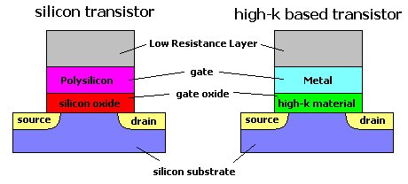
The Penryn processor debuted Intel’s 45nm fabrication, and was the first to utilize high-k gate dielectrics and metal gate electrodes. This change in technology was significant for a number of reasons:
- the processes used were far in advance of Intel’s competition
- it provided a basis on which Intel could build and scale down still further
- high-k dielectrics and metal gates allow decreases in transistor size and power consumption, and increases in speed and efficiency
As transistors get smaller the thickness of the silicon dioxide (Gate Oxide on the diagram below) needs to reduce in order to increase capacitance. Increased capacitance means increased current and improved performance, while reduced transistor size means more transistors on a die. More transistors on a die means more computing power.
Processor technology means that getting smaller and working faster and more efficiently complement perfectly.
The problem arises when the thickness of silicon decreases past a certain level and it gets so small that current begins to leak out. The electrons undergo a process known as tunnelling: they escape the transistor and dissipate which means the gate is less efficient, resulting in increased power consumption and reduced reliability. This loss in efficiency is one of the reasons chips (think later Pentiums) that had many transistors crammed onto them would produce such high TDP.
After a certain point further reduction in size becomes impractical, the physical limit of Moore’s law is reached, and a new approach is needed. Enter high-k dielectrics.

A high-k dielectric is a material with a high dielectric constant (k) which, in this case, replaces the silicon dioxide layer of the transistor. A higher dielectric constant means a greater capacitance at greater thicknesses (as compared with silicon oxide). A thicker gate oxide means less electron and current leakage, lower TDPs and increased reliability.
Intel announced that the 45nm high-k process produced processors that leaked five times less energy than a 65nm processor with comparable power.
Metal Gates
The relative ease of using silicon oxide meant that manufacturers avoided using other materials for many years in microchip manufacture. Finally, when the physical limits of manufacture using silicon oxide were quickly approaching, the change was borne out of necessity. As necessary as it was, however, Intel used the change in technologies to its advantage.
Manufacturing a transistor’s gate electrode using polysilicon was much easier than introducing a different (more efficient) material into the fabrication process. The metal gates used in the Penryn processor broke this tradition. The high-k gate oxide layer that Intel implemented on the Penryn was not compatible with a polysilicon gate electrode, so the change also meant further improvements in performance and reductions in current leakage due to the more efficient way in which the metal gates transfer current.
The efforts made to significantly improve on the materials and fabrication processes used in CPU manufacture meant that Moore’s law continued to be a prophecy.
- Principles of CPU architecture – logic gates, MOSFETS and voltage
- Basic structure of a Pentium microprocessor
- Microprocessor Evolution
- IA-32 (Intel Architecture 32 ) – base instruction set for 32 bit processors
- Pentium P5 microarchitecture – superscalar and 64 bit data
- Pentium Pro (P6) 6th generation x86 microarchitecture
- Dual Independent Bus (DIB) – frontside and backside data bus CPU architecture
- NetBurst – Pentium 4 7th generation x86 CPU microarchitecture
- Intel Core – 8th generation CPU architecture
- Moore’s Law in IT Architecture
- Architecture Manufacturing Process
- Copper Interconnect Architecture
- TeraHertz Technology
- Software Compatibility
- IA-64 Architecture
- Illustrated guide to high-k dielectrics and metal gate electrodes