Every chip has a base layer of transistors, with layers of wiring stacked above to connect the transistors to each other and, ultimately, to the rest of the computer. The transistors at the first level of a chip are a complex construction of silicon, metal, and impurities precisely located to create the millions of minuscule on-or-off switches that make up the brains of a microprocessor. Breakthroughs in chip technology have most often been advances in transistor-making. As scientists kept making smaller, faster transistors and packing them closer together, the interconnect started to present problems.

Aluminium had long been the conductor of choice, but by the mid-1990s it was clear that it would soon reach the technological and physical limits of existing technology. Pushing electrons through smaller and smaller conduits becomes harder to do – aluminium just isn’t fast enough at these new, smaller sizes. Scientists had seen this problem coming for years and sought to find a way to replace aluminium with one of the three metals that conduct electricity better: copper, silver, or gold. However, after many years of trying, no one had succeeded in making a marketable copper chip.
All this changed in September 1998, when IBM used its revolutionary new copper interconnect technology to produce a chip which used copper wires, rather than the traditional aluminium interconnects, to link transistors. It was immediately apparent that this seemingly minor change would have significant repercussions for future processor designs. Copper interconnects promised the ability to shrink die sizes and reduce power consumption, while allowing faster CPU speeds from the same basic design.
IBM has historically been renown for its lead in process technology, but has often failed to capitalise on it commercially. This time it has implemented the technology rapidly, first announcing the 0.18-micron CMOS 7SF Damascus process at the end of 1997. Subsequent development was by a four-company alliance which included fabrication equipment manufacturer Novellus Systems and, in 1999 IBM offered the 7SF process to third parties as part of its silicon foundry services.
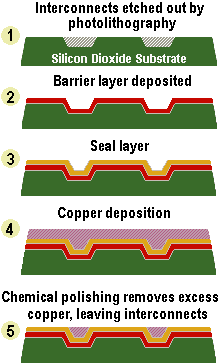
One of the problems which had thwarted previous attempts to use copper for electrical connections was its tendency to diffuse into the silicon dioxide substrate used in chips – rendering the chip useless. The secret of IBM’s new technology is a thin barrier layer, usually made from refractory titanium or tungsten nitride. This is applied after the photolithographic etching of the channels in the substrate. A microscopic seed layer of copper is deposited on top of this to enable the subsequent copper layer, deposited over the whole chip by electroplating, to bond. Chemical polishing removes surplus copper.
- Principles of CPU architecture – logic gates, MOSFETS and voltage
- Basic structure of a Pentium microprocessor
- Microprocessor Evolution
- IA-32 (Intel Architecture 32 ) – base instruction set for 32 bit processors
- Pentium P5 microarchitecture – superscalar and 64 bit data
- Pentium Pro (P6) 6th generation x86 microarchitecture
- Dual Independent Bus (DIB) – frontside and backside data bus CPU architecture
- NetBurst – Pentium 4 7th generation x86 CPU microarchitecture
- Intel Core – 8th generation CPU architecture
- Moore’s Law in IT Architecture
- Architecture Manufacturing Process
- Copper Interconnect Architecture
- TeraHertz Technology
- Software Compatibility
- IA-64 Architecture
- Illustrated guide to high-k dielectrics and metal gate electrodes
This was first invented at TI 1995, look it up.
Provide a source so we can. From all research done this article is accurate. “All this changed in September 1998, when IBM used its revolutionary new copper interconnect technology to produce a chip which used copper wires”. IBM was the first to use copper interconnect technology to produce a chip that used copper wires.