Although most of the industry agrees that Rambus is an inevitable stage in PC development, PC133 SDRAM is seen as a sensible evolutionary technology and one that confers a number of advantages that make it attractive to chip makers unsure of how long interest in Direct RDRAM will take to materialise. Consequently, in early 1999, a number of non-Intel chipset makers decided to release chipsets that supported the faster PC133 SDRAM.
PC133 SDRAM is capable of transferring data at up to 1.6 GBps – compared with the hitherto conventional speeds of up to 800 MBps – requires no radical changes in motherboard engineering, has no price premium on the memory chips themselves and has no problems in volume supply. With the scheduled availability of Direct RDRAM reportedly slipping, it appeared that Intel had little option than to support PC133 SDRAM, especially given the widespread rumours that chipset and memory manufacturers were working with AMD to ensure that their PC133 SDRAM chips will work on the fast bus on the forthcoming K6-III processor.
At the beginning of 2000, NEC begun sampling 128MB and 256MB SDRAM memory modules utilising the company’s unique performance-enhancing Virtual Channel Memory (VCM) technology, first announced in 1997. Fabricated with an advanced 0.18-micron process and optimised circuit layout and compliant with the PC133 SDRAM standard, VCM SDRAMs achieve high-speed operation with a read latency of 2 at 133MHz (7.5ns) and are package-and pin-compatible with standard SDRAMs.

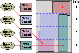
The VCM architecture increases the memory bus efficiency and performance of any DRAM technology by providing a set of fast static registers between the memory core and I/O pins, resulting in reduced data access latency and reduced power consumption. Each data request from a memory master contains separate and unique characteristics. With conventional SDRAM multiple requests from multiple memory masters can cause page trashing and bank conflicts, which result in low memory bus efficiency. The VCM architecture assigns virtual channels to each memory master. Maintaining the individual characteristics of each memory master’s request in this way enables the memory device to be able to read, write and refresh in parallel operations, thus speeding-up data transfer rates.
Continuing delays with Rambus memory as well as problems with its associated chipsets finally saw Intel bow to the inevitable in mid-2000 with the release of its 815/815E chipsets – its first to provide support for PC133 SDRAM.
- What is Level 1 (L1) Cache Memory?
- What is L2 (Level 2) cache memory?
- RAM or Main Memory – PC / computer memory (DIMM, DRAM, SDRAM)
- DRAM – Dynamic Random Access Memory
- FPM DRAM
- EDO (Extended Data Out) and BEDO (Burst Extended Data Out) DRAM
- SDRAM
- PC133 SDRAM
- DDR SDRAM explained
- DDR2 DRAM
- Dual Channel DDR Memory
- 1T SRAM
- Direct DRAM
- SIMMs
- DIMM Memory
- RIMMs Memory
- Memory Presence Detection
- Parity Memory
- ECC Memory
- Memory Upgrades
- The Evolution of Memory
- Flash Memory
- Magnetic RAM