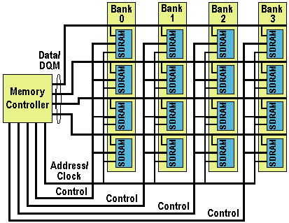
The more recent Synchronous DRAM memory works quite differently from other memory types. It exploits the fact that most PC memory accesses are sequential and is designed to fetch all the bits in a burst as fast as possible. With SDRAM an on-chip burst counter allows the column part of the address to be incremented very rapidly which helps speed up retrieval of information in sequential reads considerably. The memory controller provides the location and size of the block of memory required and the SDRAM chip supplies the bits as fast as the CPU can take them, using a clock to synchronise the timing of the memory chip to the CPU’s system clock.
This key feature of SDRAM gives it an important advantage over other, asynchronous memory types, enabling data to be delivered off-chip at burst rates of up to 100MHz. Once the burst has started all remaining bits of the burst length are delivered at a 10ns rate. At a bus speed of 66MHz SDRAMs can reduce burst rates to 5/1/1/1. The first figure is higher than the timings for FPM and EDO RAM because more setting up is required for the initial data transfer. Even so, there’s a theoretical improvement of 18% over EDO for the right type of data transfers.

However, since no reduction in the initial access is gained, it was not until the release of Intel’s 440BX chipset, in early 1998, that the benefit of 100MHz page cycle time was fully exploited. However, even SDRAM cannot be considered as anything more than a stop-gap product as the matrix interconnection topology of the legacy architecture of SDRAM makes it difficult to move to frequencies much beyond 100MHz. The legacy pin function definition – separate address, control and data DQM lines – controlled by the same clock source leads to a complex board layout with difficult timing margin issues. The 100MHz layout and timing issues might be addressed by skilful design, but only through the addition of buffering registers, which increases lead-off latency and adds to power dissipation and system cost.
Beyond 100MHz SDRAM, the next step in the memory roadmap was supposed to have been Direct Rambus DRAM (DRDRAM). According to Intel, the only concession to a transition period was to have been the S-RIMM specification, which allows PC100 SDRAM chips to use Direct RDRAM memory modules. However, driven by concerns that the costly Direct RDRAM would add too much to system prices, with the approach of 1999 there was a significant level of support for a couple of transitionary memory technologies.
- What is Level 1 (L1) Cache Memory?
- What is L2 (Level 2) cache memory?
- RAM or Main Memory – PC / computer memory (DIMM, DRAM, SDRAM)
- DRAM – Dynamic Random Access Memory
- FPM DRAM
- EDO (Extended Data Out) and BEDO (Burst Extended Data Out) DRAM
- SDRAM
- PC133 SDRAM
- DDR SDRAM explained
- DDR2 DRAM
- Dual Channel DDR Memory
- 1T SRAM
- Direct DRAM
- SIMMs
- DIMM Memory
- RIMMs Memory
- Memory Presence Detection
- Parity Memory
- ECC Memory
- Memory Upgrades
- The Evolution of Memory
- Flash Memory
- Magnetic RAM