Conspicuous by its absence from Intel’s launch of MMX at the beginning of 1997 was a 200MHz version of the Pentium MMX for notebooks. This omission was addressed before the year was out, however, with the announcement of its latest mobile processor codenamed Tillamook, after a small town in Oregon. The new processors were originally available at speeds of 200MHz and 233MHz – with a 266MHz version following early in 1998.
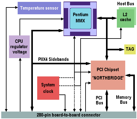
The Tillamook was one of the first processors to be built on an Intel-developed pop-out Mobile Module for notebooks, called MMO. The module held the processor, 512KB of secondary cache, a voltage regulator to buffer the processor from higher voltage components, a clock, and the new 430TX PCI Northbridge chipset. It was connected to the motherboard by a single array of 280 pins, similar to the Pentium II’s SEC cartridge.
On the chip itself, the biggest difference was in the 0.25-micron process: down from 0.35 microns in the older-style mobile Pentium chips, and much smaller than the 0.35-micron process used on desktop Pentiums. The lower micron value had a knock-on effect on the speed and the voltage.
As the transitions (the electrical pulses of ones and zeros) occurring on the processor are physically closer together, the speed is automatically increased. Intel claimed a performance increase of 30%. As the transitions are closer together, the voltage has to be reduced to avoid damage caused by a strong electrical field. Previous versions of the Intel mobile Pentium had 2.45V at the core but on Tillamook this was reduced to 1.8V. A voltage regulator was needed to protect the chip from the PCI bus and the memory bus, both of which ran at 3.3V.
The mobile 200MHz and 233MHz CPUs generated 3.4 watts and 3.9 watts TDP (thermal design power) typical respectively. These improvements represented nearly a 50% decrease in power consumption over the previous generation 166MHz mobile Pentium processor with MMX technology. This was just as well, as many of the notebooks using this chip were driving energy-sapping 13.3in and 14.1in screens intended for graphics-intensive applications. On the plus side, a lower voltage also meant lower heat emissions – a real problem with desktop chips.
The processor was sold to manufacturers either on its own in a Tape Carrier Package (TCP) format, or mounted on a Mobile Module (MMO). The module held the processor, 512KB of L2 cache, a VRM to buffer the processor from higher voltage components, a clock, and the new 430TX PCI Northbridge chipset. The module was connected to the motherboard by a single array of 280 pins, just as on the Pentium II’s SEC cartridge.

There were various reasons for putting the chip on a module. From an engineering point of view, it made it easier to combat the two main problems which arose in the area around the processor; namely heat and connections. The voltage regulator and the lower voltage of the chip helped dissipate the heat. A temperature sensor was located right by the processor, which triggered whatever heat dissipation method the manufacturer had built in. The 430TX chipset then bridged the gap between the processor and the other components, communicating with a second part of the chipset on the motherboard which controlled the memory bus and other controllers such as the graphics and audio chips.
Intel maintained that the MMO made life easier for the notebook OEMs, which could now devote more time to improving the other features of notebooks rather than having to spend too much R&D time and effort on making their systems compatible with each new processor. And, of course, as most processors required a new chipset to support their functionality, manufacturers were spared the dual problem of redesigning motherboards for the purpose and of holding obsolete stock when the new processors came in.
On the flipside, it neatly cut off the route for Intel’s competitors by forcing notebook OEMs to go with Intel’s proprietary slot. However, the much-vaunted idea that the module meant easy upgrading for the consumer was little more than wishful thinking. In practice, it was far more complicated than just opening up the back and slotting in a new SEC, as in a Pentium II desktop. Its size was also a downside. At 4in (101.6mm) L x 2.5in (63.5mm) W x 0.315in (8mm) H (0.39in or 10mm high at the connector), the module was too bulky to fit into the ultra-slim notebooks of the day.
January 1999 saw the family of mobile Pentium processors with MMX technology completed with the release of the 300MHz version.