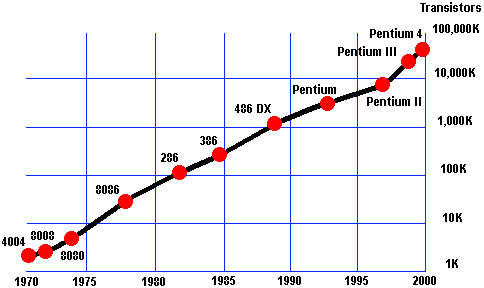
According to Moore’s Law formulated in 1965 by Gordon Moore, co-founder of Intel), the number of transistors per integrated circuit would double every 18 months. Moore predicted that this trend would hold for the next ten years. In fact, as the graph illustrates, Intel has managed to doggedly follow this law for far longer. In 1978 the 8086 ran at 4.77MHz and had less than 30,000 transistors. By the end of the millennium the Pentium 4 had a staggering 42 million on-chip transistors and ran at 1.5GHz.

The laws of physics limit designers from increasing the clock speed indefinitely, and although clock rates go up every year, this alone wouldn’t give the performance gains we’re used to. This is the reason why engineers are constantly looking for ways to get the processor to undertake more work in each tick of the clock. One approach is to widen the data bus and registers. Even a 4-bit processor can add together two 32-bit numbers, but this takes lots of instructions, whereas a 32-bit processor could do the task in a single instruction. Most of today’s processors have a 32-bit architecture, but 64-bit variants are on the way.
In the early days, processors could only deal with integers, or whole numbers. It was possible to write a program using simple instructions to deal with fractional numbers, but it would be slow. Virtually all processors today have instructions to handle floating point numbers directly.
To say that things happen with each tick of the clock underestimates how long it actually takes to execute an instruction. Traditionally, it took five ticks – one to load the instruction, one to decode it, one to get the data, one to execute it and one to write the result. In this case it is evident that a 100MHz processor would only be able to execute 20 million instructions per second.
Most processors now employ pipelining, which is rather like a factory production line. One stage in the pipeline is dedicated to each of the stages needed to execute an instruction, and each stage passes the instruction on to the next stage when it is finished with it. This means that at any one time, one instruction is being loaded, another is being decoded, data is being fetched for a third, a fourth is actually being executed and the result is being written for a fifth. With current technology, one instruction per clock cycle can be achieved.
Furthermore, many processors now have a superscalar architecture. This means that the circuitry for each stage of the pipeline is duplicated, so that multiple instructions can pass through in parallel. 1995’s Pentium Pro, for example, was able to execute up to five instructions per clock cycle.
- Principles of CPU architecture – logic gates, MOSFETS and voltage
- Basic structure of a Pentium microprocessor
- Microprocessor Evolution
- IA-32 (Intel Architecture 32 ) – base instruction set for 32 bit processors
- Pentium P5 microarchitecture – superscalar and 64 bit data
- Pentium Pro (P6) 6th generation x86 microarchitecture
- Dual Independent Bus (DIB) – frontside and backside data bus CPU architecture
- NetBurst – Pentium 4 7th generation x86 CPU microarchitecture
- Intel Core – 8th generation CPU architecture
- Moore’s Law in IT Architecture
- Architecture Manufacturing Process
- Copper Interconnect Architecture
- TeraHertz Technology
- Software Compatibility
- IA-64 Architecture
- Illustrated guide to high-k dielectrics and metal gate electrodes