Of the pair of desktop CPUs announced in the autumn of 2003, the Athlon 64 was aimed at the mass market while the top-of-the range, limited-availability Athlon 64 FX-51 model was specifically targeted at gamers and technophiles.
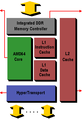
Continuing with the now familiar AMD model numbering system, the Athlon 64 3200+ boasted a clock speed of 2GHz, a little less than the FX-51’s 2.2GHz. The CPUs differ physically too, the FX-51 effectively being a higher clocked 940-pin Opteron while the mainstream part used a 754-pin form factor. The functional components of the CPU core are common to both desktop processors, one of its most significant architectural features being the integration of the system memory controller hub (MCH) into the processor itself.
This means that motherboard’s no longer need a separate Northbridge chip. Furthermore, with it now redundant, the concept of the FSB also disappears, along with the system bottlenecks it creates. Instead, the K8 architecture uses serial HyperTransport links to connect the CPU to external chips such as a Southbridge, AGP controller or another CPU. This allows the memory controller to run at the full speed of the processor. While this is still 400MHz, the integration leads to reduced latencies and increased memory performance.
|
 |
|
|
|
It is in this area that another difference between the Athlon 64 and FX-51 is to be found. While the former has a single-channel 64-bit on-die memory controller, the latter boasts the same 128-bit dual-channel memory controller as found on an Opteron processor.
The original intention had been for the Athlon 64 to have a 512KB L2 cache, the same as the Athlon XP. However, the delays in its launch and the more advanced competition it was therefore up against resulted in that being increased to an impressive 1MB. This is the principal reason for the greatly increased transistor count, up to 106 million from the Athlon XP Barton core’s 54 million. The processor is built at AMD’s Dresden, Germany wafer fabrication facility and uses 0.13 micron manufacturing technology. A new model – codenamed San Diego – based on a 0.09 process technology is expected in the first half of 2005.
The AMD64 instruction set, x86-64 – AMD’s extension to Intel’s x86 – is incompatible with the instructions of Intel’s IA-64 architecture, as supported by their Itanium server processor range. However, its big advantage – and one that AMD is pushing very hard – is 100% backwards compatibility with 32-bit x86, as supported by all Intel and AMD desktop processors.
On the same day that that AMD unveiled the Athlon 64, Microsoft announced the beta availability of a Windows XP 64-Bit Edition for 64-Bit Extended Systems which ran natively on AMD Athlon 64 processor-powered desktops and AMD Opteron processor-powered workstations. Whilst this will provide support for all existing 32-bit applications, 32-bit hardware device drivers will first need to be updated and recompiled. If the Athlon 64 were to prove a success in the consumer market Intel might find itself in the somewhat uncomfortable position of having to launch a K8-style chip itself and of having to face the indignity of having to adopt the AMD64 extensions to enable it to run Microsoft’s Windows XP 64-Bit Edition itself!
This is precisely what happened in early 2004 when Intel announced that future LGA775 based Prescott CPUs would include 64-bit x86 extensions that were compatible with AMD’s 64-bit architecture. However, any pleasure that AMD might have taken at Intel having to reverse-engineer some of its technology for a change is likely to have been short-lived as a consequence would be that AMD’s 64-bit processor line would now be forced to compete on price alone, rather than technology.
In the summer of 2004, AMD introduced the Socket 939 processor packaging, and in so doing signalled the convergence of the platforms for the mainstream and high-end desktop Athlon 64 processors. The principal difference between Socket 939 and the previous Socket 754 is that the former has a dual-channel 128-bit memory controller. As well as doubling the throughput between an Athlon 64 CPU and main memory, this also allows the use of unbuffered memory in a dual channel configurations with either an Athlon 64 or an Athlon 64 FX processor. With Socket 940, dual-channel operation of the high-end CPU had required the use of marginally slower, more expensive and less readily available registered memory.
A further advantage of the new CPU interface is the increased speed of the HyperTransport link, through which the the processor communicates with the rest of the system. Socket 939 allows a maximum bandwidth of 8GBps, compared to the previous 6.4GBps.
Apparently AMD had originally planned to release the Athlon 64 on Socket 939, but the new architecture wasn’t ready in time. Of the three new CPUs announced as the same time as the new socket interface, the mid-range 3700+ was to be the last chip to use the Socket 754 packaging. The 3500+ and 3800+ enjoyed the benefits of the new architecture, but only the then flagship FX-53 was endowed with all of those benefits – 2.4GHz clock speed, 1MB Level 2 cache 1,000MHz HyperTransport link and dual-channel memory controller.
Given AMD’s track record of changing CPU interfaces only rarely, Socket 939 was expected to remain the consumer market platform for the foreseeable future. Socket 940 will revert to its originally intended role of workstation/server platform, with the single channel Socket 754 appearing destined to become the platform for the budget sector.