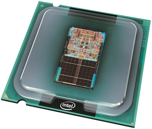
The Intel Core 2 Duo processor family announced on 27 July 2006 consists of five desktop PC processors, tailored for business, home and enthusiast users, and five mobile PC processors designed to fit the needs of a mobile lifestyle. The desktop part comprises around 291 million transistor on a die of 143mm2. It’s packaged in a LGA775-style socket and runs on a 1066MHz FSB.

Ever since the introduction of its K8 microarchitecture, and its on die memory controller, AMD has had a performance advantage over Intel. The principal reason for this is the huge reduction in memory latency that results from the fact that communication does not have to go via the Northbridge. Intel have chosen not to follow suit in their Core 2 processors, preferring to use any additional on-die transistors to increase the Level 2 cache to 4MB. As well as allowing greater flexibility with respect to supporting additional memory types (it was a considerable time before AMD’s memory controller moved from DDR to DDR2 memory), it is also consistent with the Intel Core microarchitecture’s emphasis on efficiency, since cache does consume less power.
Indeed, the power consumption of the new Core 2 processors is extremely low, with claimed TDPs of 65 watts for Conroe and most Woodcrests, 80 watts for the 3.0 GHz Woodcrest, and 40 watts for the low-voltage Woodcrest. Merom, the mobile variant, is listed at 35 watts TDP for standard versions and 5 watts TDP for Ultra Low Voltage (ULV) versions. Moreover, according to Intel the reduction in power consumption is achieved at the same time as an increase in performance:
- 20% more performance for Merom at the same power level (compared to Core Duo)
- 40% more performance for Conroe at 40% less power (compared to Pentium D)
- 80% more performance for Woodcrest at 35% less power (compared to the original dual-core Xeon)
Intel’s solution to the memory latency issue has been to introduce a number of minor improvements in the Core microarchitecture, which combine to achieve a significant hike in overall system performance. The table below, which compares the mobile Core 2 Duo processor and its closest relation, the Core Duo predecessor, identifies several of these incremental improvements:
| Core 2 Duo (Merom) | Core Duo (Yonah) | |
|---|---|---|
| Manufacturing Process | 65nm | 65nm |
| Die Size | 143mm2 | 90mm2 |
| Transistors | 291 million | 151 million |
| Clock Speeds | 1.06GHz – 2.4GHz+ | 1.20GHz – 2.33GHz |
| FSB Frequency | 533MHz – 800MHz | 533MHz – 667MHz |
| L1 Cache Size | 32KB + 32KB | 32KB + 32KB |
| L2 Cache Size | 2MB – 4MB Shared | 2MB Shared |
| Pipeline Stages | 14 | 12 |
| Decoders | 1 complex + 3 simple | 1 complex + 2 simple |
| Maximum Decode Rate | 4+1 | 3 |
| Reorder Buffer | 96 | 80 |
| SSE Units | 3 | 1 |
| Socket Interface | Socket-M (PGA/BGA)
Socket-P (PGA/BGA) |
Socket-M (PGA/BGA) |
The slightly deeper pipeline enables increased clock speeds and techniques such as memory disambiguation and improved prefetch logic also help offset any advantage an integrated memory controller offers. Overall, while AMD’s approach to reducing memory latency is arguably simpler and more elegant, the improvements implemented in the Intel Core 2 chips make them undeniably the more efficient processors, able to decode and process more instructions per clock cycle than CPUs based on the K8 microarchitecture.
The expectation was for the following desktop line-up to begin shipping in early August 2006:
| Processor | Frequency | Bus Speed | L2 Cache |
|---|---|---|---|
| Intel Core 2 Extreme processor X6800 | 2.93 GHz | 1066 MHz | 4MB |
| Intel Core 2 Duo processor E6700 | 2.66 GHz | 1066 MHz | 4MB |
| Intel Core 2 Duo processor E6600 | 2.40 GHz | 1066 MHz | 4MB |
| Intel Core 2 Duo processor E6400 | 2.13 GHz | 1066 MHz | 2MB |
| Intel Core 2 Duo processor E6300 | 1.86 GHz | 1066 MHz | 2MB |