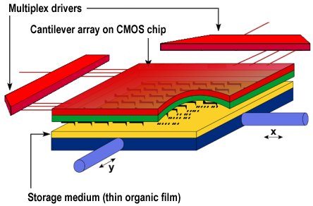
In late 1999, IBM’s Zurich Research Laboratory unveiled a concept which suggests that micro- and nanomechanic systems may be able to compete with electronic and magnetic devices in the mass storage arena. Instead of writing bits by magnetising regions of a disk’s surface, Millipede – as the scientists have nicknamed their novel device – melts tiny indentations into the recording medium’s surface.
Based on Atomic Force Microscopy, the technology uses tips mounted on the ends of tiny cantilevers etched in silicon to scan surfaces in minute detail. Millipede’s tips are heated with electric pulses to 750 degrees F (400 degrees C), hot enough to melt the disk’s polymer-film surface. The tips leave holes just 30 to 50 nm across. Each hole represents a bit. To read the data, Millipede detects whether a tip is in a hole by taking the cantilever’s temperature.
The most recent array design consists of an array of 64 x 64 cantilevers (4096) on a 100 µm pitch. The 6.4 x 6.4 mm2 array is fabricated on a 10 x 10 mm2 silicon chip using a newly developed transfer and join technology that allows the direct interconnection of the cantilevers with CMOS electronics used to control the operation of the cantilevers. With this technology the cantilevers and CMOS electronics are fabricated on two separate wafers, allowing the processes used in the fabrication to be independently optimised. This is a critical feature, as many of the processes used to fabricate mechanical structures such as cantilevers are not compatible with the fabrication of CMOS electronics.
The cantilevers used in the array are of a three-terminal design, with separate heaters for reading and writing, and a capacitive platform for electrostatic actuation of the cantilevers in the z-direction. The cantilevers are approximately 70 µm long, with a 500-700 nm long tip integrated directly above the write heater. The apex of each tip has a radius on the scale of a few nanometers allowing data to be written at extremely high densities (greater than 1 Tbits/in2). In addition to the cantilevers, the array chip also carries eight thermal sensors which are used to provide x/y positioning information for closed-loop operation of the micro-scanner.

High data rates can be achieved by parallel operation of a large number of tiny tips in a small area. IBM scientists believe their technique will eventually allow storage densities of up to 500 gigabits per square inch (80 Gbit/cm2). That’s five to ten times the presumed upper limit for magnetic storage.
- Hard disk (hard drive) construction
- Hard Disk (hard drive) Operation
- Hard disk (hard drive) format – the tracks and sectors of the hard disk
- File systems (FAT, FAT8, FAT16, FAT32 and NTFS) explained
- Hard Disk (Hard Drive) Performance – transfer rates, latency and seek times
- Hard Disk AV Capability
- Hard Disk Capacity
- Hard Disk Capacity Barriers
- Hard Disk MR Technology
- Hard Disk GMR Technology
- Hard Disk Pixie Dust
- Hard Disk Longitudinal Recording
- Hard Disk Perpendicular Recording
- RAID – Redundant Arrays of Inexpensive Disks
- Hard Disk SMART Drives
- Hard Disk MicroDrives
- Hard Disk OAW Technology
- Hard Disk PLEDM
- Hard Disk Millipede
- Guide to Western Digital’s GreenPower hard drive technology
- Solid state hard drive (SSD) technology guide