Polymers are chemical substances that consist of large molecules that are, themselves, made from many smaller and simpler molecules: proteins and DNA are examples of naturally occurring polymers; many others, such as nylon, are artificially created. Because of their flexibility and strength, polymers are used for products such as car bumpers and bullet-proof vests.
Conjugated polymers had already found favour as conductors in battery electrodes, transparent conductive coatings, capacitor electrolytes and through-hole plating for double-sided circuitboards. Then, in 1989, researchers from Cambridge University’s Cavendish Laboratory discovered that certain conjugated polymers could be made to emit light in addition to carrying electric current. The idea of developing a display device using these properties soon followed and LEP’s developer and patent holder – Cambridge Display Technology (CDT) – was born.
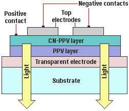
As described previously, the LEP display is closely related to the humble LED, indeed, sometimes being referred to as polyLED. However, whereas the LED’s light producer is a traditional semiconductor material, LEP uses a two-layer polymer – a hole-transporting layer of poly(p- phenylene vinylene) (PPV) and an emissive layer of a cyano-substituted PPV derivative (CN-PPV) – to achieve the same effect. When electrons and holes – flowing in opposite directions between two electrodes – meet, the electrons drop into the holes and release its extra energy as light. The greater the difference in energy between the hole and the electron; the further from red and the closer to blue the light given off. Not surprisingly, early displays produced by CDT were closer to the red end of the spectrum than the blue and it wasn’t until late-1999 that the company announced the development of a blue-emitting polymer material and therefore the prospect of being able to produce a full-colour display.

In terms of manufacture, the polymers are extremely simple to produce, and the circuitry doesn’t need to be any more complex than that already used in LCDs. Working with ink-jet veterans Seiko Epson, CDT has developed a thin film deposition technique that involves the application of drops of treacle-like polymer liquid as small as 30 microns across onto a patterned electrode array.
Indeed, the technology has many potential advantages over LCD: only one sheet of plastic is required instead of two sheets of glass, LEPs don’t need backlights, so they consume less power, and since it’s the surface of the LEP which emits light, wide viewing angles are possible. Furthermore, not only can it be applied to very large surfaces but, since they use flexible substrates, LEP displays can be curved, and possibly even made flexible.
On the strength of these advantages CDT claims that LEP screens will replace LCDs within the next few years. The company’s exploitation route for the technology is through licensing and technology transfer, coupled with corporate partnerships, joint ventures and developments and device manufacturing. Whilst it’s still early days for LEP in terms of real products, by late-2001 licenses had already been granted to the likes of DuPont Displays, OSRAM, Philips and Seiko-Epson, some of whom had already announced imminent start of production whilst others were actively implementing their manufacturing strategies.
- VA – Vertically Aligned LCD Monitors
- What in the LCD is IPS!?
- ThinCRT Flat Panels
- TFT LCD Monitors
- LCD Resolutions and Picture Scaling
- Liquid Crystal Light Polarisation in LCD Monitors
- Polysilicon Flat Panels
- Plasma Flat Panels
- PALCD Flat Panels
- OLED Flat Panels
- MVA – Multi-domain Vertical Alignment in LCD Monitors
- LEP Flat Panels
- LED Flat Panels
- LCD – Liquid Crystal Displays
- IPS – In-Plane Switching LCD Monitors
- HAD Flat Panels
- Flat Panel Feature Comparisons
- FED Flat Panels
- Digital Flat Panels
- DSTN LCD monitors
- Creating Colour in LCD Displays
- Flat Panel ALiS Technology